- Suit #2, 2nd Floor, Khan Center, Abdali Road, Multan
- +92 321 8633444 +92 61 4580344-5
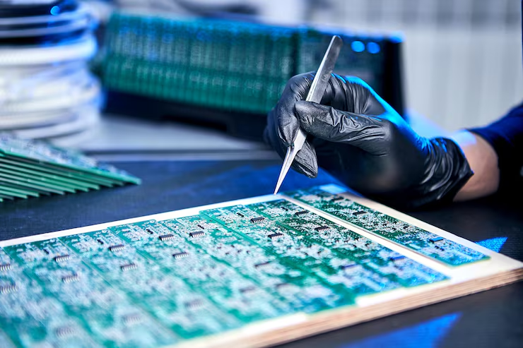
At ERC TECH, our experienced PCB design engineers provide high-quality PCB Design & Layout Services for global customers. From schematic design to layout, manufacturing support, and testing, we specialize in multi-layer, high-speed, high-density, and high-precision designs that meet the most demanding industry requirements.
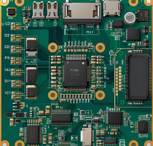
Our expertise covers HDI, rigid-flex PCBs, FPC, high-speed backplanes, A/D designs, SI/PI simulation, EMC/EMI design, and more. Whether for aerospace, medical, automotive, telecommunications, or consumer electronics, we deliver optimized PCB layouts that ensure performance, reliability, and manufacturability.
A well-designed PCB is the foundation of a reliable electronic product. Our team balances electrical performance, heat management, mechanical strength, and aesthetics to ensure designs that are not only functional but also cost-effective and production-ready. By minimizing signal interference, optimizing component placement, and ensuring manufacturability, ERC TECH reduces development risks and accelerates time-to-market.
We follow a proven, step-by-step design workflow: schematic capture → PCB layout → rule definition and DFM check → footprint creation → routing → verification and analysis → Gerber generation. Every stage is documented and reviewed to ensure quality and compliance.
With ERC TECH, PCB design isn’t just about connections on a board — it’s about creating the foundation for high-performance, reliable, and scalable electronic products.